Also called monolayer graphene, single-layer graphene
van der Waals crystalsemimetal
The material that started the field: a single sheet of carbon atoms that conducts electricity and heat exceptionally well, is nearly transparent, and is the strongest material ever measured. It cannot switch fully off the way a silicon transistor must, so its realistic future is in sensors, photonics, heat spreading and composites rather than in logic chips.
Crystal structure
Drag to turn
Three layers of Bernal (AB) graphite, the usual form. The middle layer is shifted so that half its atoms sit over atoms of the layer below and half over the centres of hexagons; the third layer lines up with the first again. Layers 3.36 Å apart, c = 6.71 Å. Cell from Trucano and Chen, Nature 258, 136 (1975); COD 9011577.
Three layers of rhombohedral (ABC) graphite, a minority form in natural graphite. Each layer is shifted by the same step in the same direction, so the pattern repeats only after three layers. Thin flakes of it have flat electronic bands, which is why rhombohedral multilayers are studied alongside twisted graphene. Cell from Lipson and Stokes, Proceedings of the Royal Society A 181, 101 (1942); COD 1200018, layers 3.35 Å apart.
C
Cell
Hexagonal, a = 2.46 Å
Atoms per cell
2
C–C bond
1.42 Å
Height
Flat: one atomic plane
Each carbon atom bonds to three neighbours, and the bonds close into hexagons. The dashed outline is one unit cell. It holds two atoms, one on each of the two triangular sublattices, A and B. Lattice constant 2.46 Å, the in-plane value of graphite.
What it looks like
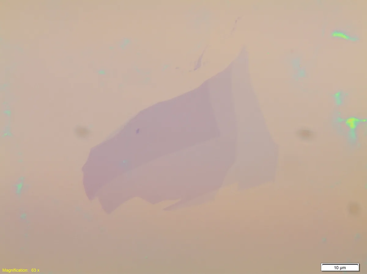
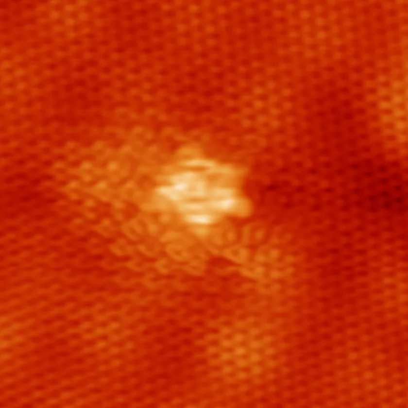
A flake peeled from graphite and pressed onto an oxidised silicon wafer, in an optical microscope. The shade changes in steps with the thickness, which is how the thinnest regions are found. Scale bar: 10 µm. Image: Harlequin Mantis, CC BY-SA 4.0; resized.Graphene grown on silicon carbide, imaged with a scanning tunnelling microscope. The fine regular pattern follows the carbon lattice; the bright patch is a single point defect. Image: Nathan Guisinger, Argonne National Laboratory, public domain; resized.
Key properties
Room-temperature mobility above 100,000 cm2/(V·s) in hBN-encapsulated devices; typically 2,000–15,000 cm2/(V·s) on SiO2
Fermi velocity ≈ 1 × 10⁶ m/s, about 1/300 of the speed of light
Intrinsic strength ~130 GPa and Young’s modulus ~1 TPa (AFM nanoindentation of suspended flakes)
Thermal conductivity ~2,000–5,000 W/(m·K) for suspended monolayers at room temperature; the spread reflects measurement method
Absorbs 2.3% of white light per layer (πα)
Theoretical specific surface area 2,630 m2/g
How it is made
Mechanical exfoliation of graphite – highest quality, micrometre-scale flakes; the reference material for physics
CVD on copper foil at ~1,000 °C – continuous polycrystalline films, roll-to-roll capable, but must be transferred
Silicon sublimation from SiC above ~1,300 °C – transfer-free wafer-scale films; the basis of graphene quantum resistance standards
Liquid-phase or electrochemical exfoliation – tonnes of few-layer flakes for inks, coatings and composites
Epitaxy on single-crystal Cu(111) or Cu–Ni foils – single-orientation wafer-scale films, research to pilot stage
Uses, and how close they are
Composites, coatings and conductive inks (as few-layer flakes)deployed
Hall-effect magnetic field sensorsdeployed
Quantum Hall resistance standards (epitaxial graphene on SiC)deployed
Modulators and photodetectors on silicon photonicsprototype
Field-effect biosensors and neural interfacesprototype
Readiness runs lab → prototype → pilot → deployed.
Open problems
Can single-crystal graphene be transferred at 300 mm scale without cracks, wrinkles and polymer residue – or grown directly on the target substrate at CMOS-compatible temperatures?
Once grain boundaries are eliminated, what limits room-temperature mobility in large-area films: wrinkles, strain fluctuations or residual charged impurities?
Is there a way to open a technologically useful band gap without sacrificing the carrier mobility that made graphene attractive?
Going deeper
Short notes for specialists. Choose a lens in the header and yours comes first.
For theoreticians · your lens
The textbook Dirac system: nearest-neighbour tight binding with t ≈ 2.7–3.0 eV reproduces the low-energy bands, and DFT places the Dirac cone correctly, but electron–electron interactions renormalise the Fermi velocity logarithmically towards charge neutrality – GW captures this, semilocal DFT does not. Flexural (ZA) phonons with quadratic dispersion dominate heat transport and make computed thermal conductivity strongly size- and strain-dependent. Most of the open physics has moved into stacks: see twisted and rhombohedral graphene.
For experimentalists · your lens
Find monolayers by optical contrast on 90 nm or 285–300 nm SiO2 and confirm with Raman: a single Lorentzian 2D band near 2,680 cm−1 (532 nm excitation) with a FWHM of ~25–30 cm−1, and I(2D)/I(G) above 2 in undoped samples; the D band near 1,350 cm−1 reports defects. Both G and 2D shift with strain and with doping, so separate the two with a G–2D correlation plot. For device quality, clean dry transfer and hBN encapsulation matter more than where the graphite came from.
For engineers · your lens
The missing band gap limits graphene FETs to on/off ratios of about ten at room temperature, which rules out digital logic. Graphene wins where fast carriers, an all-surface channel or transfer-free growth on SiC matter: RF, photonics, sensing and metrology. The practical bottlenecks are transfer yield, contact resistance (typically a few hundred Ω·µm, best reports near 100 Ω·µm) and doping variation from process residues.
First Graphene has entered a three-year Development and Commercialization Agreement with Turkish prepreg manufacturer Aeropreg to bring a PureGRAPH®-enhanced carbon fiber prepreg to market. The agreement pairs First Graphene's proprietary epoxy concentrates, developed to optimize how PureGRAPH® graphene is incorporated…
In the temperature interval T∼50 - 100 K, the rate of electron-electron collisions in graphene devices may exceed the momentum relaxation rate due to disorder and electron-phonon scattering. In this regime, the motion of the electron liquid may be described by the hydrodynamic equations. In the hydrodynamic…
A central goal of the emerging field of materials QED is to harness subwavelength electromagnetic confinement in engineered cavities to tailor light-matter interactions. Here, we demonstrate that van der Waals multilayer cavities composed of stacked graphene and hexagonal boron nitride (hBN) provide unprecedented…
We theoretically investigate the optical response of the WSe2 monolayer vertically stacked on twisted bilayer graphene (tBG) under electrostatic doping. In this heterostructure, the doped moiré superlattice of tBG generates a spatially modulated electrostatic potential that couples to the electron and hole constituents…
Periodically strained graphene provides a versatile platform to realize moiré-like electronic structures. We show that the interplay between strain-induced pseudomagnetic field and a displacement-field-controlled scalar potential enables the formation of isolated narrow bands. Some of the low-energy bands are…
Electric field effect in atomically thin carbon filmsNovoselov et al. · Science 306, 666 (2004)cited by 67,052doi:10.1126/science.1102896
The electronic properties of grapheneCastro Neto et al. · Reviews of Modern Physics 81, 109 (2009)cited by 24,886doi:10.1103/RevModPhys.81.109
Measurement of the elastic properties and intrinsic strength of monolayer grapheneLee et al. · Science 321, 385 (2008)cited by 20,948doi:10.1126/science.1157996