A 2D material is a crystal that is one atom thick and still holds together. Pull a single layer out of a stack and it stops behaving like the block it came from: graphite is the soft grey solid you write with, and one layer of it is the strongest material anyone has ever measured and carries heat better than any metal. Computer screens of known crystals suggest more than a thousand could be thinned this way, and the ones that have been tried often change character when you do it – some start glowing, some become superconducting, some become magnets. The interesting question is no longer whether the physics is strange, which is settled, but which of these properties survive contact with a factory.
About 55 minutes to read in fullEvery section stands on its ownRevised 4 Oct 2026
A is a solid that exists as a stable sheet one atom – or a few atoms – thick. Inside the sheet, atoms are held together by strong , the same kind that make diamond hard. Between one sheet and the next there are no such bonds, only a weak stickiness, the same faint attraction that makes a gecko’s foot cling to glass. This is why the sheets can be prised apart at all, and why a single sheet does not fall to pieces once it is on its own. Graphite in a pencil is millions of these sheets stacked one on another; graphene is one of them.
Inside each layer, atoms are joined by strong chemical bonds. Between layers there is only a weak attraction, which is why a single layer can be lifted off. In graphite the layers sit 0.335 nm apart.
How thin is thin?
Layers in graphite sit 0.335 nanometres apart. A sheet of ordinary office paper is about 0.1 millimetres thick, which is 100,000 nanometres. Divide one by the other: you would need about 300,000 sheets of graphene stacked up to match the thickness of one sheet of paper. Turn it around and it gets stranger. A graphene one millimetre across – large by the standards of the field – is three million times wider than it is thick. Blow it up until it is as thick as that sheet of paper and it would be 300 metres across, about three football pitches laid end to end. And it would still be a single unbroken crystal.
A sheet of office paper 0.1 mm
A human hair about 70 µm
A red blood cell about 8 µm across
A bacterium about 2 µm long
A wavelength of green light about 530 nm
A flu virus about 100 nm
The DNA double helix about 2 nm wide
One layer of MoS20.65 nm
One layer of graphene 0.335 nm
1 mm100 µm10 µm1 µm100 nm10 nm1 nm0.1 nm
Each step along the scale is ten times smaller than the one before. From a sheet of paper to one layer of graphene is more than five of those steps: a factor of about 300,000.
How we got here
For most of the twentieth century, physicists had a good argument that a one-atom-thick crystal could not exist on its own. Every atom in a solid jiggles, and the warmer it is the more it jiggles. In a normal three-dimensional crystal the neighbours on all sides hold each atom roughly in place. In a sheet with nothing above or below, the argument went, the up-and-down jiggling adds up without limit across the sheet, until the atoms wander far enough that the crystal stops being a crystal – it should crumple, roll up or fall apart. The argument was correct as far as it went, and the escape clause turned out to be mundane: real sheets are not perfectly flat.
They ripple gently in the third dimension, and those ripples stiffen the sheet, the way corrugating cardboard stiffens it. And the destabilising effect grows so slowly with the size of the sheet that it never becomes decisive for flakes of any size anyone can make. In 2004, Andre Geim and Konstantin Novoselov at the University of Manchester peeled layers off a lump of graphite with sticky tape, dropped them on an oxidised silicon , found them under an optical microscope and measured electricity flowing through them. The point was less that a existed than that it was easy – the material could be made on a bench in an afternoon and it did not fall apart.
Each dot is one milestone, stacked by decade. 5 came in the 145 years before 2004, 23 in the 21 years since. Point at a dot for the event, or select it to jump to the entry below.
1859
Benjamin Brodie, working in Oxford, treats graphite with strong acids and oxidants and reports a new carbon compound he calls graphic acid, what we now call graphite oxide.
Why it mattered
The chemistry that peels graphite apart is over 160 years old. Nearly all graphene made in bulk today still descends from this reaction, which is a useful corrective to the idea that this field began in 2004.
1947
Philip Wallace calculates the of a single layer of graphite as a mathematical step towards understanding bulk graphite.
Why it mattered
The strange result, that the electrons behave as if they have no mass, was on paper 57 years before anyone had a sheet to test it on. For Wallace the single layer was simply a theoretical starting point.
1962
Hanns-Peter Boehm and colleagues in Germany examine reduced graphite oxide in an electron microscope and identify flakes so thin they are likely single layers.
Why it mattered
Strong evidence for isolated monolayers existed decades before the Nobel-winning work. The 2004 breakthrough was not first sight of graphene but the first time anyone could measure what a sheet actually did electrically.
1966
Robert Frindt cleaves molybdenum disulfide crystals into layers only a few molecules thick using adhesive tape.
Why it mattered
The sticky-tape method that later made graphene famous was already being used on a different layered material, and the 2D family was never only about carbon.
1986
Boehm and co-authors propose the name graphene for a single layer of graphite in a formal nomenclature paper.
Why it mattered
The name arrives twenty years before the material becomes a research field, and its origin is a committee on carbon terminology rather than a discovery announcement.
2004
Andre Geim and Konstantin Novoselov in Manchester isolate graphene with adhesive tape, put it on an oxidised silicon wafer and show its conductivity can be switched with a .
Why it mattered
This is the paper that started the field. The critical trick was not the tape but the choice of thickness, which made a single atomic layer visible under an ordinary optical microscope so that flakes could be found and wired up.
2005
Two groups independently show that electrons in graphene behave like relativistic particles, through measurements of an unusual .
Why it mattered
It converted graphene from a curiosity into a testbed for fundamental physics, and made a table-top experiment capable of probing questions that previously required particle accelerators.
2008
Columbia researchers press a diamond tip into a suspended graphene sheet and measure its strength; a separate study finds a single sheet absorbs about 2.3 percent of visible light.
Why it mattered
These produced the two numbers that dominate popular coverage: strongest material ever measured, and almost perfectly transparent. Both are accurate, and both apply only to a flawless flake a few micrometres across.
2009
Researchers grow large-area graphene films on copper foil by .
Why it mattered
Tape does not scale. Growing graphene from methane gas on a metal surface was the first route to sheets big enough for real devices, and it is still the dominant method for high-quality film.
2010
A Korean team demonstrates production and transfer of a 30-inch graphene film for a touch screen.
Why it mattered
It showed that graphene could be made continuously, like newspaper, and set the expectation that graphene touchscreens were imminent. Graphene touchscreens never became a mainstream product, which makes this both a technical milestone and a lesson in how far a demonstration is from a product.
2010
Geim and Novoselov receive the Nobel Prize in Physics for groundbreaking experiments regarding the two-dimensional material graphene.
Why it mattered
Six years from first paper to Nobel is extraordinarily fast. It also triggered a funding surge and a wave of publicity whose promises the field has been living with ever since.
Two groups show that molybdenum disulfide changes its electronic character when thinned to a single layer, becoming a strong light emitter.
Why it mattered
Graphene conducts too well to switch off, which makes it a poor digital . This showed that other 2D materials are proper , redirecting the field from carbon towards the .
2011
A group at Drexel University discovers by chemically aluminium out of a layered ceramic, producing a , water-dispersible 2D material.
Why it mattered
It opened a whole family, now numbering dozens of compositions, that conducts like a metal and can be processed as an . MXenes underpin most of the serious work on 2D and energy storage.
2011
A team in Lausanne builds a working transistor from a single layer of molybdenum disulfide with a high- .
Why it mattered
It demonstrated a 2D transistor that switches properly on and off, which graphene cannot do. Every industrial 2D electronics programme traces back to this result.
2013
The European Union launches the Graphene Flagship, a ten-year research programme with a budget in the region of one billion euros.
Why it mattered
It was one of the largest research initiatives Europe had ever funded on a single material, and it set an explicit goal of moving graphene from laboratory to factory. Its record is mixed and worth examining rather than celebrating.
2013
Researchers demonstrate that graphene in hexagonal boron nitride and contacted only along its exposed one-dimensional edge gives dramatically better electrical quality.
Why it mattered
It solved, for research purposes, both the contamination problem and part of the contact problem. Almost every high-quality 2D physics result since, including , depends on this technique. It has not been industrialised.
2015
The National Graphene Institute opens in Manchester at a cost of about 61 million pounds.
Why it mattered
It marked the peak of the era in which governments built graphene buildings. The scientific output has been strong; building an industry around the research has proved much slower than building the research capacity.
2017
Two independent groups show that magnetism survives in materials only one or two atomic layers thick.
Why it mattered
Long-standing theory suggested should be destroyed by thermal fluctuations in two dimensions. Finding otherwise opened magnetic 2D materials as a field, though the temperatures involved were far below room temperature.
2017
Samsung’s research institute publishes a graphene ball material claimed to allow much faster charging and greater capacity in cells.
Why it mattered
It was widely reported as the arrival of the graphene battery. No commercial cell based on it has been announced since, and it stands as a clean example of a real, peer-reviewed result that never became a product.
2017
Two groups make the first 2D crystals, replacing the atoms on one face of a molybdenum disulfide or diselenide sheet so that its top and bottom are different elements (MoSSe).
Why it mattered
It showed that the two faces of a single atomic sheet can be engineered separately. The mismatch builds an electric field into the crystal itself – a property with no counterpart in an ordinary crystal of the same atoms, and of interest for , and -based electronics.
2018
A team at MIT shows that two graphene sheets stacked with a relative twist of about 1.1 degrees become superconducting.
Why it mattered
It created the field of twistronics, in which the angle between two layers becomes a design parameter. It is widely seen as one of the most important 2D results since 2004, and it has no application yet, working only within a couple of degrees of absolute zero.
2018
A study tests material sold as graphene by 60 producers worldwide and concludes that quality is generally poor and that most companies are really producing graphite microplatelets.
Why it mattered
It was the field’s most useful embarrassment. It confirmed publicly that the word graphene on a datasheet meant very little, and it strengthened the case for the standards work that followed.
2021
Paragraf, a University of Cambridge spin-out, is selling graphene sensors grown directly on wafers without a transfer step.
Why it mattered
It is the clearest case of a commercial electronic device in which the 2D material is the working part rather than an additive. The volumes are small and the market is instrumentation, not consumer electronics.
2021
The first international standard defining how to characterise graphene-related materials is published, following years of unreliable commercial material.
Why it mattered
Standards are boring and they are how a material becomes an industry. Buyers could finally specify what they were purchasing, which matters more for commercialisation than most laboratory results.
2023
The Graphene Flagship’s ten-year programme comes to an end, having produced a large body of research, several spin-outs and no mass-market product built on graphene.
Why it mattered
It is the clearest data point available about the pace of this field. A billion euros and a decade of coordinated European effort moved 2D materials from physics into early industry, but not into consumer products, and the reasons are structural rather than a failure of effort.
2023
Several groups observe the effect in twisted layers of molybdenum ditelluride: electrons collectively behave as if carrying fractions of their charge, with no magnetic field applied.
Why it mattered
States like this previously required magnetic fields of many tesla. Finding one in a twisted 2D stack at zero field is among the clearest signs that stacking produces physics no bulk crystal offers, and theoreticians have proposed such states as a possible route to more robust quantum bits.
2024
A graphene brain interface is used in a human patient for the first time, placed temporarily on the brain surface during tumour surgery in Manchester as part of a study.
Why it mattered
It moved 2D materials into clinical medicine, the field with the most demanding evidence requirements of any application on this list. It is a safety trial, which is the beginning of a long road, not the end of one.
2025
A team at Fudan University reports WUJI, a 32-bit RISC-V microprocessor built from 5,900 molybdenum disulfide transistors.
Why it mattered
It is the largest working 2D logic chip demonstrated – the previous record was 115 transistors – and it is about as complex as a commercial microprocessor from the mid-1970s. That comparison is the point: it shows both real progress and the size of the remaining gap.
What is not a 2D material
Three things are routinely confused with 2D materials.
A thin film is not a 2D material.
Films of metal or oxide a few nanometres thick have been evaporated onto surfaces for a century. Their thickness is a dial that can be set anywhere, they have chemically unsatisfied bonds sticking out of the top surface, and thinning them further makes them worse – they break up into islands. A 2D material has no dial: it is one layer, or two, or three, and each is a different material.
A nanoparticle is not a 2D material.
A nanoparticle is small in all three directions; a 2D sheet is small in exactly one and can be centimetres across in the other two.
Graphite is not graphene.
It is the same atoms in the same arrangement, just many layers of it, and the extra layers change the physics: stack about ten layers of graphene and the electronic behaviour has already converged back to that of ordinary graphite. This matters commercially. Much of what is sold as graphene is graphite ground very fine – platelets tens of layers thick – which is a useful material, but not the same one.
Why thin changes everything
8 things change when a crystal is thinned to a single layer. Each comes with an everyday picture.
01
Squeeze an electron and you change its energy
An electron in a solid is not a dot; it is a spread-out wave, and in a typical semiconductor that wave is a few nanometres wide.
Read moreShow less
Make the material thinner than the wave is wide and the wave has to be squashed to fit. Squashing it costs energy, and it costs more the harder you squash. So the energies an electron is allowed to have shift upwards, and the gaps between allowed energies get wider. This is not a small effect at these thicknesses. The of molybdenum disulfide – the property that decides what colour light it absorbs and emits – goes from about 1.2 electronvolts in the bulk crystal to about 1.9 in a single layer. That is the gap light sees; freeing an electron altogether costs a few tenths of an electronvolt more, for the reason explained in 06 below. The chemistry has not changed; only the thickness has.
Everyday picture
A guitar string. Press it against a fret and you shorten the string; the note goes up. You have not changed the string, the tension or the player – only how much room the wave has, and the pitch follows. Nor can you get any note you like out of it: a string of a given length allows certain notes and not others, and that is exactly the situation an electron in a thin sheet is in.
A wave squeezed into less room sits higher in energy, as a string pressed against a fret sounds a higher note (a sketch, not to scale). The right-hand side is to scale: in molybdenum disulfide the gap that sets the colour of light it absorbs and emits widens from about 1.2 eV in the bulk crystal to about 1.9 eV in a single layer. Band gap in the glossary →
02
There is no inside – every atom is a surface atom
Take a one-centimetre cube of silicon. Roughly one atom in ten million sits on its surface; all the rest are buried.
Read moreShow less
That is why bulk semiconductors tolerate a dirty world: contamination is a skin complaint, and the skin is a vanishing fraction of the patient. A single layer has no skin and no interior. Every atom is exposed to whatever is above and below it. This cuts both ways. It makes 2D materials extraordinary sensors, because a handful of gas molecules landing on a sheet measurably changes its resistance. It also means the substrate underneath is not a passive shelf but part of the material. Put graphene on ordinary oxidised silicon and its electrons scatter off trapped charges in the oxide; put the same graphene on a flake of boron nitride, which is atomically smooth and chemically inert, and how freely the electrons move improves by roughly a factor of ten.
Layers
Thickness
Atoms at a surface
Only the top and bottom layers touch the outside, so in a stack of N layers they hold 2 in N of the atoms. The layers here are graphite’s, 0.335 nm apart; at a centimetre, about 30 million layers, the share is about 1 in 15 million, close to the silicon cube’s one in ten million.
Everyday picture
A swimming pool and a puddle. Tip a teaspoon of ink into the pool and nothing visible happens; the volume swallows it. Tip the same teaspoon into a puddle and the puddle is now the colour of the ink. A bulk crystal is the pool. A monolayer is the puddle – which makes it a terrible material to be careless with and a superb one to measure things with.
03
Nothing is left hanging, so anything stacks on anything
This is the biggest change, and it helps to see exactly what it replaced.
Read moreShow less
Cut a silicon crystal and the atoms at the cut have bonds that end in mid-air, chemically desperate for a partner. To grow a second semiconductor on top, its atoms must sit almost exactly where silicon’s bonds expect them – the two crystals’ atomic spacings must match to roughly one percent. Germanium is chemically silicon’s closest relative and its spacing is about four percent bigger; grow it directly on silicon beyond a very thin layer and the tears the interface into a mat of defects. That single constraint shaped semiconductor engineering for fifty years.
It is why gallium arsenide devices are built on gallium arsenide wafers, why entire industries organised themselves around a handful of compatible material families, and why many devices that were obvious on paper were never built. A 2D crystal has no bonds pointing out of its face. All bonds are satisfied within the sheet. So when you lay one sheet on another they are not chemically joined at all – they simply stick, by the same weak attraction that holds the layers of graphite together. Nothing has to line up. You can stack a conductor on an insulator on a light emitter on a magnet, in any order, at any rotation, whether or not their atoms are spaced alike. The constraint did not get easier. It stopped applying.
Everyday picture
Growing a conventional semiconductor on another is like laying interlocking tiles: each tile has to drop into the pattern below, so the two patterns must be the same size or the floor buckles. Stacking 2D layers is like laying sheets of paper on a desk. Nothing interlocks. They stay put because they are flat and slightly sticky, and it makes no difference whatsoever what is printed on the sheet underneath.
A typical stack, built one sheet at a time on a substrate: hBN underneath for a flat, clean base, two different semiconductors in the middle – one of them turned by a small angle – and an hBN cover lowered on top to seal it. No layer has to match its neighbour’s lattice, because nothing bonds across the interfaces. Van der Waals heterostructure in the glossary →The numbers from the text: bonded crystals must match their atomic spacings to roughly 1%, so germanium, about 4% bigger than silicon, grown on it beyond a very thin layer tears the interface into defects. Stacked sheets are not bonded to each other, so their spacings need not match at all.
04
The material suddenly switches on the light
Silicon has powered computing for sixty years and has never made a decent light source, which is why the laser in a fibre-optic transmitter is not made of silicon.
Read moreShow less
The reason is a mismatch. When an electron in silicon falls to a lower energy state it must also change its momentum, and a particle of light carries almost none, so the electron needs a lattice vibration to arrive at the same instant and take up the difference. Three things must coincide, which is rare, so the electron usually gives up its energy as heat instead. Molybdenum disulfide has the same problem in bulk. Thin it to a single layer and the squashing described above rearranges the allowed energies so the mismatch disappears: the electron can drop straight down and emit light on its own. The result is dramatic and easy to see – the same material, thinned from two layers to one, glows enormously more brightly. This is how a monolayer is routinely identified in a lab: shine a laser on it and see whether it answers.
Everyday picture
A step you can walk down, versus a step where you must also hop sideways onto a moving walkway at the exact moment your foot lands. Most people do not manage the second one and stand at the top instead. Thinning the crystal removes the walkway.
Energy against momentum for an electron in molybdenum disulfide (a sketch). In the bulk crystal the lowest empty state and the highest filled one (the two dots) sit at different momenta, so the electron can only fall with a lattice vibration arriving at the same moment. In a single layer the two line up and it drops straight down, giving off light. Photoluminescence in the glossary →
05
Extremely strong, and yet you can roll it up
These usually trade off against each other. Graphene does not make the trade, and the reason is geometry rather than magic.
Read moreShow less
Pulling on a sheet means stretching carbon-carbon bonds directly, and those are among the strongest bonds in chemistry, which is why a defect-free patch of graphene withstood about 130 gigapascals before breaking – roughly a hundred times the strength of high-strength structural steel. Bending is a different matter entirely. When you bend a sheet, the outer face stretches and the inner face compresses, and how much that costs depends on how far apart those two faces are.
In a monolayer they are the same atoms. Bending costs essentially nothing. So the sheet is nearly unbreakable in-plane and nearly free to fold, which is exactly the combination a flexible or wearable device wants. The caveat is the one that always applies: that 130 gigapascals was measured by pushing a needle into a perfect flake a few micrometres across. Real material has holes, edges and , and it is the holes that break.
Everyday picture
A steel girder and a strand of steel wool are the same steel. You cannot bend the girder with your hands; the strand wraps round your finger. Nothing about the metal changed – only how far the outside of the bend is from the inside.
Left, a sketch: bending a thick sheet stretches its outer face and squeezes its inner one, and the further apart the faces, the more that costs. In a single layer both faces are the same atoms, so it bends almost for free. Right, to scale: a defect-free patch of graphene withstood about 130 gigapascals, roughly a hundred times high-strength structural steel – measured by pressing a needle into a perfect flake a few micrometres across; real sheets break at their holes and edges.
06
Electrons stop hiding from each other
When an electron is knocked out of place in a solid it leaves behind an empty spot with the opposite charge, and the two attract.
Read moreShow less
In a bulk crystal, the atoms packed all around them partly cancel that attraction, the way a crowd muffles a conversation. The pair is barely bound: in silicon the binding is about fifteen thousandths of an electronvolt, in gallium arsenide only about four, and ordinary room-temperature jiggling supplies about twenty-six, so the pair is torn apart the moment it forms. In a single layer, most of the electric field between the two charges does not travel through the material at all.
It arcs through the empty space above and below the sheet, where there is nothing to cancel it. The binding jumps to a few tenths of an electronvolt – more than ten times room-temperature jiggling – so these pairs survive at room temperature and dominate how the material absorbs and emits light. It also means electrons in these sheets feel each other strongly rather than gliding past independently, and strongly interacting electrons are where the unexpected behaviour lives: magnetism, superconductivity, states of matter with no bulk equivalent.
Everyday picture
Two people trying to hold a conversation across a packed party, versus across the same room after everyone has gone home. Same distance, same voices. The difference is entirely in what is in between.
The same electron–hole pair in two settings. In a bulk semiconductor the surrounding crystal screens their attraction, so the pair is large and easily broken. In a monolayer most of the field lines between them pass through the vacuum or substrate around the sheet, where little screens them, so the pair is small and strongly bound. Exciton in the glossary →The numbers from the text, on a logarithmic scale: an electron and its hole in silicon are bound by about 0.015 eV, less than the about 0.026 eV of room-temperature jiggling, so the pair falls apart. In a single layer the binding is a few tenths of an electronvolt, drawn here as 0.3 to 0.5 eV.
07
Three knobs that do not exist in a bulk crystal
In a conventional semiconductor the important properties are fixed when the crystal is grown.
Read moreShow less
Impurities are baked in at high temperature and stay where they are put. With 2D materials, three things can be changed after the fact, on a finished device. Voltage: because the sheet is thin enough to be influenced all the way through, a nearby electrode can change the number of mobile electrons in it by orders of magnitude, and in some stacks flip the material between insulating, metallic and superconducting behaviour.
Strain: monolayers have been stretched by several percent without breaking, where a silicon wafer typically cracks below about one percent, and a few percent of stretch measurably shifts the colour of the light the material emits. Twist: because stacked layers are not chemically bonded, one can be rotated relative to the other. In 2018 a group at MIT found that two graphene sheets rotated to about 1.1 degrees – and only near that angle – become superconducting when cooled. Neither sheet does anything of the kind alone.
as many mobile electrons as with the knob at zero
silicon cracks
a silicon wafer survives this too
1.1°
moiré period 4.7 nm; no superconductivity
Three settings a finished 2D device can still change. Voltage alters how many electrons are free to move, here over two orders of magnitude. A monolayer takes several percent of stretch; a silicon wafer typically cracks below about 1%. Twisting two graphene sheets makes a moiré pattern whose period is the lattice constant, 0.246 nm, divided by 2 sin(θ/2); near 1.1°, and only there, the pair superconducts when cooled.
Everyday picture
A bulk semiconductor is baking: once the cake is out of the oven the recipe is settled and you can only decorate. A 2D stack is closer to a mixing desk – the sliders are still there after the recording is made, and moving one changes what the material is, not just how it is packaged.
08
In graphene, electrons behave as if they weigh nothing
In an ordinary metal or semiconductor, an electron’s energy rises as the square of how fast it is going, the same way a car’s kinetic energy does.
Read moreShow less
In graphene it rises in a straight line – which is the relationship a particle of light obeys, and light has no mass. So graphene’s electrons act like massless particles that always travel at the same speed, about a million metres per second. That is fast, but it is only about one three-hundredth of the speed of light, which makes graphene a rare thing: a benchtop material in which effects normally associated with high-energy physics can be measured with a voltmeter. Practically, it is part of why current flows through clean graphene so freely, with electrons travelling micrometres without hitting anything. It is also the origin of graphene’s most awkward commercial fact. That straight-line relationship has no gap in it, and a gap is precisely what a transistor needs in order to switch fully off.
Everyday picture
Most things get harder to speed up the faster they go. A massless particle does not: it has one speed and always moves at it, and giving it more energy makes it more energetic without making it faster. Graphene’s electrons took the second option, which is not something electrons in copper are entitled to do.
Left: in an ordinary semiconductor the bands curve, and a gap separates them. Right: in graphene the filled and empty bands are two cones that touch at a single point. Their sides are straight, so every electron near the tip moves at the same speed, about 106 m/s, whatever its energy. Dirac cone in the glossary →
How they are made
8 ways to make a 2D material, from sticky tape to wafer-scale furnaces. Every route trades quality against quantity, and each has a limit worth knowing.
Top-down · 3
Start from a layered crystal and take layers off it.
Top-down routes can only use a layered crystal that already exists, and they give flakes, powders or inks, never a continuous sheet – but tape gives the best material there is, and liquid exfoliation the most, by the tonne. Bottom-up routes grow a film where it is wanted, up to whole wafers, at the cost of grain boundaries or of a transfer onto the surface you actually need. Select a method for how it works and where it stops.
Sticky tape
mechanical exfoliation
Press adhesive tape onto a crystal of graphite, or molybdenum disulfide, or any of a few hundred other layered crystals.
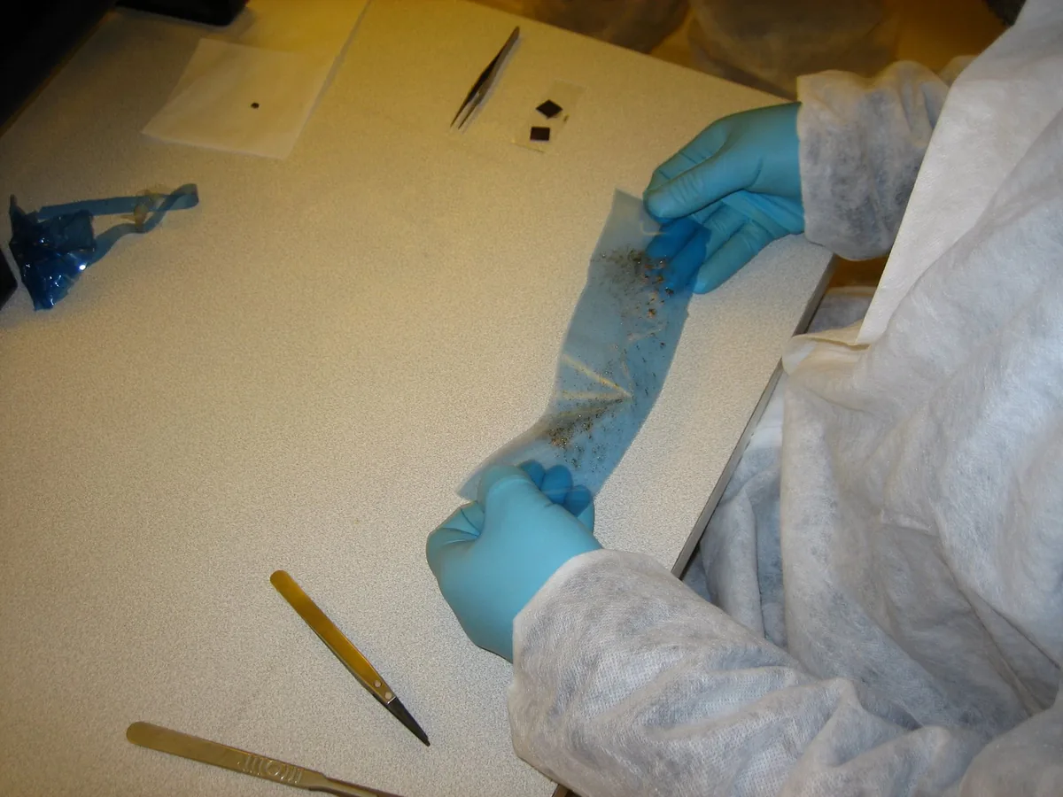
Peeling graphite apart on adhesive tape. The grey specks are flakes of graphite, and each time the tape is folded and pulled apart they get thinner. Image: Alexander Mayorov, CC BY-SA 3.0; resized.
Everyday pictureSplitting a slate roof tile with a knife, except the tile splits at every level and you keep going until nothing is left to split.
Read moreShow less
Peel. Fold the tape onto itself and peel again, repeatedly, halving the thickness each time. Press the tape onto a silicon wafer with a precisely chosen thickness of oxide on it and the thinnest flakes become faintly visible under an ordinary optical microscope, because a single atomic layer changes the interference colour of the reflected light just enough for the eye to catch. Then you hunt for them.
How far it has scaled
Typical usable flakes are tens of micrometres across – a fraction of a millimetre. Variants that first bond a freshly deposited metal layer, usually gold, to the crystal – so that the top layer clings to the metal more strongly than to the layer below – have lifted off single layers millimetres to centimetres across.
Where it stops
This will not scale to manufacturing. Most of what lands on the tape is too thick, and the useful flakes have to be found one at a time under a microscope; robots now do the searching and can stack the flakes they find, but every sample remains a one-off. It survives because it produces the highest-quality material in existence: flakes torn straight out of a crystal, with no growth defects and no chemical residue. Most of what is known about 2D physics was measured on tape-made samples, and reference measurements are still made this way.
Liquid-phase exfoliation
Put graphite powder in a suitable liquid and shear it violently – with ultrasound, a high-shear mixer, or a machine that forces the mixture through a narrow gap at high pressure.
Everyday pictureShuffling a deck of cards so hard the cards separate, then keeping them apart by suspending them in syrup.
Read moreShow less
The turbulence slides layers off each other. Choose a liquid whose surface energy nearly matches the material’s and the separated flakes stay suspended rather than clumping back together. Spin off the thick bits and you have an ink. One widely cited scale-up study even did the shearing in an ordinary kitchen blender.
How far it has scaled
This is the only route currently producing 2D carbon materials by the tonne; industrial plants are rated in hundreds to thousands of tonnes per year of graphene-related powder. Individual flakes are typically under a micrometre across and several layers thick.
Where it stops
It makes powder and ink, never a continuous sheet. That suits , coatings, inks and battery additives; printed circuits made from networks of flakes work too, but current has to hop from flake to flake, so they fall far short of devices made from a . The output is inherently a mixture – a distribution of flake sizes and layer counts rather than a single product – and the thicker end of that distribution is in fact fine graphite. This is where most of the industry’s quality problems come from.
Chemical vapour deposition
CVD
Put a metal foil, usually copper, in a furnace at around 1000 degrees Celsius and flow a carbon-bearing gas such as methane over it.
Everyday pictureFrost forming on a cold window. Nobody places the crystals; the conditions make them grow, they spread outwards from wherever they started, and where two growth fronts meet you can see the seam.
Read moreShow less
The gas breaks apart on the hot metal surface, carbon atoms skate around and lock into a hexagonal sheet. Copper is chosen because carbon barely dissolves in it, so growth stops when the surface is covered – the process is largely self-limiting at one layer. The film then has to be lifted off the copper and moved onto whatever substrate the device needs, usually by gluing a polymer to the top, dissolving or delaminating the copper away, and floating the film onto the target.
How far it has scaled
Continuous roll-to-roll growth and transfer of graphene film was demonstrated at 30-inch diagonal scale, and later work produced continuous films metres long. Layered semiconductors such as molybdenum disulfide have been grown as continuous monolayers on 200 and 300 millimetre wafers in industrial research fabs.
Where it stops
The growth is largely solved; the transfer is not. Peeling the film off its catalyst and floating it onto another surface introduces tears, wrinkles, polymer residue and trapped bubbles, and it is the single biggest gap between laboratory graphene and industrial graphene. The films are also polycrystalline – many small grains meeting at boundaries that scatter electrons – so a large CVD sheet performs worse than a small tape-made flake.
Growing the bulk crystal first
vapour transport, flux or melt
Seal the elements – molybdenum and sulfur, say – in an evacuated quartz tube with a small amount of a such as iodine, and put the tube in a furnace with one end hotter than the other.
Everyday pictureGrowing sugar crystals on a string in a jar, but driven by a temperature difference across the jar rather than by evaporation, and taking a fortnight.
Read moreShow less
The transport agent picks up material at the hot end as a vapour, carries it down the tube and releases it at the cold end, where it crystallises slowly over days or weeks. Two other routes do the same job: in the crystal grows out of a molten bath, often of one of its own elements, as it cools slowly; in a melt is frozen from one end. The product is not a 2D material at all. It is a beautifully ordered bulk layered crystal, which is then exfoliated by one of the other methods.
How far it has scaled
Bulk crystals millimetres to a few centimetres across. The highest-quality hexagonal boron nitride, grown by a different, high-pressure, high-temperature method at Japan’s National Institute for Materials Science, is supplied to research groups worldwide and functions as a de facto standard for the field.
Where it stops
This is a for research, not a manufacturing route. It is slow, batch-based, and produces a three-dimensional crystal that still has to be taken apart afterwards. Its importance is that the very best 2D device results still start from a bulk crystal grown first – for many transition metal dichalcogenides now by flux growth, which leaves fewer defects than vapour transport – a striking dependency for a field that talks about scale.
Molecular beam epitaxy
MBE
Inside a chamber pumped to a vacuum better than that of low Earth orbit, heat the constituent elements in separate crucibles so they evaporate as thin beams of atoms.
Everyday pictureSpray-painting a wall one atom at a time, in a room so clean that a stray molecule of air counts as vandalism, while an inspector counts every layer as it lands.
Read moreShow less
Aim the beams at a heated substrate and open shutters to control precisely how much of each arrives. Growth proceeds slowly enough that a single atomic layer takes minutes, and instruments watch the surface in real time as it builds.
How far it has scaled
Wafer-scale films are routine for conventional semiconductors; for 2D materials the films cover the wafer but are usually made of small crystalline domains rather than one continuous crystal.
Where it stops
Unmatched control, poor throughput. A machine costs several million euros and growth is measured in hours per wafer, which is acceptable for research and for a few high-value products and hopeless for anything commodity. For 2D semiconductors, crystal quality achieved so far generally trails what chemical vapour deposition produces, which is an uncomfortable result for the more expensive technique.
Etch-and-delaminate
how MXenes are made
Start with a bulk ceramic built of alternating layers – a titanium-aluminium carbide, for instance.
Everyday pictureDissolving the mortar out of a brick wall and lifting off the courses of brick one at a time. The bricks were never attacked; only the stuff between them was.
Read moreShow less
The aluminium layers are chemically weaker than the rest. Soak the powder in a fluoride-containing acid and the aluminium is selectively dissolved out, leaving the titanium carbide layers behind, now held together only weakly and decorated with whatever chemical groups the etchant left on their surfaces. A gentle shake in water then separates them into single sheets. The family this produces, discovered at Drexel University in 2011, is called MXenes, and it is unusual for being both atomically thin and metallically conductive, with several dozen compositions now made.
How far it has scaled
Batches of tens of grams have been made in the laboratory, and a handful of specialist suppliers sell MXene powders and dispersions.
Where it stops
It requires hydrofluoric acid or reagents that generate it in place, which is a serious industrial hygiene problem, and milder etchants are an active research topic rather than a solved one. The product also oxidises in water and air, so shelf life is limited. And the method only works where a sacrificial layer exists to remove – it is not a general recipe.
Post-growth conversion
turn a film you already have into a 2D crystal
Rather than assembling the sheet atom by atom, deposit an ordinary film by an ordinary method and then convert it chemically.
Everyday pictureRather than baking a loaf, buying ready-made dough and proving it. The shaping happens with equipment you already have; only the final transformation is new.
Read moreShow less
Coat a wafer with a thin molybdenum or molybdenum oxide film using standard equipment, then heat it in sulfur vapour; the sulfur works its way in and reorganises the film into layered molybdenum disulfide. The attraction is that the hard part – putting a uniform film on a large wafer – is done by machines that semiconductor fabs already own and trust. The same idea, applied to a finished monolayer, produces one of the field’s stranger materials. Strip the top layer of sulfur atoms from a sheet of molybdenum disulfide and replace it with selenium, and the result is a Janus layer – named after the two-faced Roman god – whose top and bottom are different elements. Because the two faces no longer match, the sheet carries a built-in electric field across its own thickness, something no ordinary crystal of the same atoms has.
How far it has scaled
Demonstrated across full semiconductor wafers, with uniformity across the wafer as the metric that matters rather than any single flake size.
Where it stops
The conversion tends to produce many small grains rather than one crystal, and the grain boundaries hurt electrical performance in exactly the applications that motivated the approach. Getting the layer count uniform across a whole wafer is also harder than it sounds when one layer too many changes the material’s properties.
Growing graphene out of the substrate itself
epitaxial graphene on silicon carbide
Silicon carbide is a commercial semiconductor sold as polished wafers.
Everyday pictureRather than laying a lawn, burning off the topsoil until what is left underneath is already the surface you wanted.
Read moreShow less
Heat one above roughly 1300 degrees Celsius in vacuum or argon and silicon atoms leave the surface faster than carbon does. The carbon left behind rearranges into graphene, on the wafer, in place. There is no catalyst foil and no transfer step, which removes the single dirtiest part of the CVD route.
How far it has scaled
Produced on commercial silicon carbide wafers up to 150 millimetres in diameter, and this route underpins graphene-based electrical resistance standards used by national measurement laboratories.
Where it stops
Silicon carbide wafers are expensive, which caps the addressable applications to those where the substrate is affordable or already required. The graphene is also stuck to the substrate it grew from – the very thing that makes it clean makes it non-transferable – and the first carbon layer bonds to the silicon carbide and behaves differently from free graphene, which complicates the electronics.
Myths
10 things people often believe about graphene and its relatives, and what is actually true.
Say whether you had believed each one, and what is actually true opens.
Myth 01Graphene will replace silicon.
Had you believed this?
It will not, and the reason is specific rather than a matter of engineering effort.
Read moreShow less
A logic transistor has to turn off – modern chips demand that the off state pass many orders of magnitude less current than the on state, because a few billion transistors leaking slightly is a warm phone with a flat battery. Switching off requires a gap in the material’s allowed electron energies, and graphene has no gap. At room temperature its is typically ten or less.
There are ways to force a gap open – cut graphene into narrow ribbons, apply a field across two stacked layers – and every one of them sacrifices the effortless electron transport that made graphene attractive in the first place. In short, graphene is a superb conductor, a superb sensor and a superb , and a bad switch. The 2D materials with a real chance at logic transistors are the layered semiconductors such as molybdenum disulfide and tungsten diselenide, which have gaps to begin with – and even they are competing to extend silicon at the far end of miniaturisation, not to replace it.
Myth 02Graphene is already in everything.
Had you believed this?
It is in a modest and specific list of things, and in most of them it is a performance additive at low loading rather than the main event.
Read moreShow less
Sports equipment, some tyres and shoe soles, some coatings, some concrete, some battery and electrodes, thermal-management films in a few phones, and a small number of precision sensors and measurement standards. Notice the pattern: these are applications where a small addition of a relatively cheap powder measurably improves an existing product. That is a real business and it is not the same thing as the material that appears in press releases. Nothing you own contains a monolayer of graphene doing something that only a monolayer could do.
Myth 03It’s just a form of carbon, so it must be cheap.
Had you believed this?
The raw material is almost worthless; graphite is a bulk commodity mineral.
Read moreShow less
Everything expensive happens afterwards, and what you are paying for is control. Graphene nanoplatelets – the powdery, many-layered, unglamorous kind – are sold by the kilogram at industrial prices. A continuous single layer grown on a wafer costs on the order of hundreds of dollars for a few square centimetres, because it demands a high-temperature furnace, a metal catalyst, an ultra-clean transfer and inspection of every piece. The gap between those two prices is not a market inefficiency waiting to be squeezed out. It is the cost of the difference between a powder and a near-perfect crystal, and it is the same gap that separates sand from a silicon wafer.
Myth 042D means flat, and flat means simple.
Had you believed this?
Free-standing 2D sheets are never perfectly flat – they ripple, and the rippling is part of what makes them stable, so it cannot simply be engineered away.
Read moreShow less
Beyond that, removing a dimension makes the physics harder, not easier. Electrons interact more strongly rather than less, because there is less material around to screen them. behave differently in two dimensions than in three. Defects that would be diluted in a bulk crystal sit directly in the current path. And ‘flat’ hides the field’s richest variable: two flat sheets stacked at a slight angle produce a large-scale interference pattern in the atomic positions, and that pattern – not the sheets – can determine the behaviour. graphene, made of nothing but carbon, hosts superconducting, magnetic and insulating states depending on angle and voltage.
Myth 05The 2010 Nobel Prize means the science is finished.
Had you believed this?
The prize marked the start of the field rather than its conclusion, and graphene has since become the least surprising member of the family.
Read moreShow less
Superconductivity in twisted bilayer graphene was found in 2018, eight years after the prize. Magnetism in single atomic layers was reported in 2017. Entire material families now central to the field, such as MXenes, were discovered after 2010. Large-scale computational screens of known crystals have identified over a thousand candidate layered compounds that could plausibly be exfoliated, and only a small fraction have been made, let alone measured. The prize recognised that a door had been opened. Most of the rooms are still dark.
Myth 06One atom thick must mean fragile.
Had you believed this?
It is the strongest material ever measured. Thinness makes it easy to bend, which is a different property, and easy to tear from a defect, which is a third.
Read moreShow less
The right mental model is a sheet of cling film made of diamond: extraordinarily hard to stretch, trivially easy to fold, and if there is a nick in the edge it will run. That last part is why real material with grain boundaries and holes performs far below the textbook number, and why ‘strongest material ever measured’ is a true statement that has so far proved commercially difficult to cash.
Myth 07If a product says it contains graphene, it contains graphene.
Had you believed this?
This has been tested, and the answer was bad. A 2018 study in the journal Advanced Materials tested material from 60 graphene producers worldwide, using , and chemical analysis.
Read moreShow less
Its conclusion, in short: the quality of the world’s graphene was generally poor, and most companies were in fact producing graphite microplatelets – flakes many layers thick – rather than graphene. The root cause is not simply fraud. Until standards bodies pinned the definitions down, ‘graphene’ was a word with no agreed technical meaning, and a supplier selling finely milled graphite was less lying than using a word that did not yet mean anything specific. International standards now define the terms, and reputable suppliers publish characterisation data.
Myth 08Graphene and 2D materials are the same subject.
Had you believed this?
Graphene is one material out of a family. Hexagonal boron nitride looks almost identical – same , similar spacing – and is one of the best electrical insulators known, which makes it the field’s default substrate and encapsulant.
Read moreShow less
Molybdenum disulfide and its relatives are semiconductors that glow. MXenes are metallic and disperse into water-based inks. Black phosphorus has a gap that changes with layer count. Several materials are magnetic as single sheets. Graphene attracts most of the attention and most of the money, and it is arguably now the least likely member of the family to end up as the channel of a transistor.
Myth 092D materials were discovered in 2004.
Had you believed this?
Extremely thin carbon layers were reported in the 1960s, and the name ‘graphene’ was coined years before anyone isolated a flake with tape.
Read moreShow less
Molybdenum disulfide was cleaved down to a few molecular layers with adhesive tape in 1966, and single layers were made chemically in 1986. Layered minerals and the fact that they cleave have been known for centuries – that is what mica and graphite are. What 2004 changed was accessibility: a method anyone could repeat, on a substrate where the flakes could be found with a normal microscope, together with electrical measurements showing the sheet behaved as a working electronic device. Fields do not start when something is first observed. They start when it becomes easy enough that a thousand groups can join in.
Myth 10Thinner is always better.
Had you believed this?
It depends entirely on what you want. One layer of molybdenum disulfide emits light strongly and two layers barely do, so a light emitter wants exactly one.
Read moreShow less
But a single layer carries less total current than several, has no volume to store charge in, and is exquisitely sensitive to whatever it is sitting on. Battery electrodes usually work better with few-layer material, which is cheaper anyway. Thermal and structural composites do fine with platelets tens of layers thick. Bilayer graphene, unlike the monolayer, can have a gap opened by an applied voltage, which makes it more interesting for switching than its more famous single-layer cousin. ‘How many layers’ is a design parameter with an optimum, and that optimum is often not one.
Numbers that stick
0.335 nanometres
The spacing between layers in graphite
This is effectively the thickness of one sheet of graphene, and it is close to the smallest thickness any free-standing material can have, because you cannot have less than one atom. Almost every other number in this field is a consequence of this one.
About 300,000
Sheets of graphene needed to match the thickness of one sheet of paper
Counting one sheet per second, it would take you three and a half days to count the stack, and the result would be one sheet of paper.
2.3 percent
The fraction of visible light absorbed by a single layer of graphene
Small enough that graphene is nearly transparent, and enormous for something one atom thick – a monolayer absorbs far more light per atom than almost anything else. The figure is also remarkable for what sets it: it barely depends on the details of graphene at all, but on a fundamental constant of nature that governs how strongly light and matter interact everywhere in the universe. You can get at that constant with a piece of tape and a lamp.
0.77 milligrams
The mass of one square metre of graphene
The Nobel committee’s illustration remains the best one: a hammock one square metre across, made of a single layer of graphene, could in principle hold a four-kilogram cat, and the hammock itself would weigh about as much as one of the cat’s whiskers.
130 gigapascals
The measured breaking strength of defect-free graphene
Roughly a hundred times the strength of high-strength structural steel, measured on a flake small enough to contain no flaws. This is the ceiling, not the floor, and the gap between them is where all the engineering lives.
About 1.1 degrees
The twist angle at which two stacked graphene sheets become superconducting
Rotate one sheet relative to the other by roughly one degree and cool it, and a material made of nothing but carbon carries current with no resistance. Go a fraction of a degree either way and the effect is gone. It is the clearest demonstration that in this field the arrangement of the layers is an ingredient in its own right, on a par with which elements you started from.
More than 1,000
Known crystals that computation says should peel into 2D sheets
A large screen of known crystal structures – over a hundred thousand of them – flagged well over a thousand compounds as layered enough to exfoliate, with a substantial subset looking straightforward. Only a small fraction have been isolated and measured. The field’s supply of unexplored materials is nowhere near running out.
About 1 billion euros over 10 years
The European Union’s Graphene Flagship programme, 2013 to 2023
One of the largest coordinated research programmes Europe has funded, running for a full decade with hundreds of partner institutions. It is a useful yardstick for the distance between research investment and commercial return: a decade and a billion euros produced a real industrial supply chain, a standards framework and a large body of science, and did not produce a mass-market consumer product built around a monolayer. That is a fair description of where the field stands.
A crystal that is one atom thick, strongly bonded within the sheet and only weakly stuck to the sheets above and below – which is why it can be peeled apart at all, and why the single sheet holds together once it is alone.
Is graphene safe? Is it toxic?
It depends on which material, in what form, and by what route of exposure, and that the picture is incomplete. ‘Graphene’ covers everything from a pristine monolayer to an oxidised powder, and these behave very differently in the body. What is reasonably established: biological effects track flake size, layer count, surface chemistry and dose rather than the word ‘graphene’; small, well-dispersed, oxygen-rich flakes are cleared more readily than large, stiff, water-repelling ones; and the asbestos comparison fits only partly: asbestos is dangerous because immune cells cannot fully engulf long, rigid fibres, and animal studies suggest very large, stiff graphene platelets can provoke a similar frustrated response, while small flakes are handled far more easily.
A double-blind trial published in 2024, in which 14 healthy volunteers inhaled highly purified, very small graphene oxide flakes for two hours, found no effect on lung function, blood pressure, heart rate or markers of inflammation, and only a very slight change in a laboratory test of blood clotting – reassuring, but not the same as knowing about long-term, high-dose or workplace exposure. The workplace risk today is a fine-powder handling risk, managed the way other fine powders are. The consumer risk from graphene bound inside a composite is generally regarded as low, because the flakes are not free to move.
Why is it taking so long?
Three separate reasons, and it helps to keep them apart. First, materials are always slow: carbon fibre took roughly thirty years to go from laboratory curiosity to commercial aircraft structure, and lithium-ion batteries took about two decades from first reports to product. Nothing about graphene’s timeline is unusual by that standard. Second, the specific hard problem is not making the material but making it uniformly, in quantity, and getting it onto the surface where it is needed without damaging it – transfer, not growth, is the bottleneck.
Third, and most decisive: an incumbent material is not beaten by being better on one axis. Silicon is not merely a substance, it is sixty years of accumulated manufacturing knowledge, and displacing it means beating that entire system on cost, yield and reliability at once. The applications that arrive first are always the ones with no incumbent to displace.
Can I actually buy anything with graphene in it today?
Yes, in a few categories, though mostly as a small additive rather than as the main ingredient. Sports goods – tennis racquets, bicycle tyres, some running shoes – use small additions to composites or rubber. Construction: graphene-enhanced concrete has been poured in real buildings, with the claim being that less cement is needed for the same strength, which matters because cement is a large source of carbon dioxide emissions. Some phones use graphene-based films to spread heat away from the processor. Batteries and supercapacitors use graphene-related powders as conductive additives. At the high-precision end, graphene-based magnetic field sensors are sold commercially, and graphene grown on silicon carbide is used in electrical resistance standards at national measurement laboratories. What you cannot buy is a consumer device whose central working component is a single atomic layer.
Is it expensive?
There are two products under one name. Graphene-related powders and platelets are an industrial commodity sold by the kilogram, cheap enough that adding a fraction of a percent to a composite is commercially sensible – this is the material in tyres and concrete. Continuous monolayer film on a wafer is priced like a specialty semiconductor product: a few square centimetres of monolayer graphene on a substrate costs on the order of hundreds of dollars, and research-grade hexagonal boron nitride is comparably precious. Anyone quoting a single price for graphene is telling you which of the two products they sell.
Is it bad for the environment?
Producing it has a real footprint that depends heavily on the route. Chemical of graphite has classically used strong oxidising acids, generating acidic waste that must be treated. Vapour deposition means running a furnace at around 1000 degrees Celsius, and the copper catalyst is often dissolved away rather than reused. Etching MXenes involves fluoride chemistry. Per kilogram, the energy cost of high-quality graphene is far above that of bulk commodity materials.
Set against this: the quantities used in most real applications are small, and some applications are net-negative on emissions if they work – graphene-enhanced concrete that reduces cement content is the clearest example, given that cement production is responsible for something on the order of seven percent of global carbon dioxide emissions. Life-cycle assessments in this field are still thin and vary enormously by production route, so anyone who tells you confidently that graphene is green, or that it is dirty, is ahead of the evidence.
Who is winning, China or the West?
It depends what ‘winning’ counts. On volume, China leads decisively: it files the large majority of the world’s graphene patents, publishes the largest share of papers, and hosts the largest production capacity for graphene powders, backed by sustained national and provincial funding. Europe invested heavily and coherently through a ten-year, roughly one-billion-euro research programme running from 2013 to 2023, and retains particular strength in high-quality material, in measurement and standards, and in the underlying science.
The United States is strong in fundamental discovery and in the semiconductor-adjacent work that matters most for electronics. A useful caution: patent counts and paper counts measure activity, not capability, and several of the field’s most consequential results have come from small groups rather than from the largest programmes. The most decisive asymmetry is probably not in 2D materials at all but in the advanced chip manufacturing that any 2D electronics would eventually have to run on.
Did the Nobel Prize go to the right people?
It went to Andre Geim and Konstantin Novoselov in 2010, and this was contested at the time. The objections were reasonable ones. Very thin carbon layers had been reported decades earlier by other groups, and the word ‘graphene’ was coined by someone else entirely. Several researchers – working on graphene grown on silicon carbide, on chemical routes, and on the electronic measurements that revealed graphene’s most distinctive behaviour – had strong independent claims, and a Nobel Prize can be shared by at most three people. The defence is that the 2004 work did something the earlier work did not: it made single layers reliably obtainable, identifiable and measurable, and it showed that a single atomic layer worked as an electronic device. Whether that constitutes discovery or enablement is the argument, and it is a genuine one rather than a manufactured grievance.
Can I make graphene at home?
You almost certainly make a little of it every time you write with a pencil – single layers are present in pencil marks, which was true long before anyone knew it. With sticky tape, a graphite crystal and patience you can make flakes. What you cannot do at home is find them, because locating a monolayer requires putting it on a wafer with a precisely chosen oxide thickness and looking through a good optical microscope, and confirming it requires a spectrometer. Making it is easy. Knowing you made it is the expensive part – which is, in miniature, the entire industrial problem.
If graphene has no band gap, what is it actually good for?
A great deal, once you stop asking it to be a logic transistor. It is among the best thermal conductors ever measured, which makes it attractive for moving heat out of dense electronics. It is transparent – a single layer absorbs 2.3 percent of visible light – and conductive at the same time, a rare combination useful for electrodes. It is an exceptional sensor precisely because every atom is exposed. It is extremely strong and light, which suits composites. It is chemically stable and impermeable to gases, which suits barrier coatings and . It is well suited to high-frequency analogue electronics, where you want fast electrons and do not need to switch fully off. The absence of a gap rules out one application, the most famous one, and leaves the rest untouched.
Is graphene really the strongest material in the world?
By the measurement that was made, yes. A flake a few micrometres across, suspended over a hole and pushed with a diamond tip until it broke, held about 130 gigapascals – the strength of the chemical bonds themselves, on a patch too small to contain a defect. Any large sheet has grain boundaries, holes and edges and fails at the weakest of them, as every material does; graphene’s ceiling is unusually high, and so is the distance from that ceiling to what a real sheet delivers.
How many 2D materials are there?
A few dozen are studied intensively, and computer screens of over a hundred thousand known crystals flag well over a thousand more as built of layers weakly enough bound to peel apart. Only a small fraction of those have been isolated – not one wonder material but a periodic table’s worth of them, most of which nobody has yet made.
Will 2D materials end up in my phone?
Partly and unevenly. The most likely first entries are unglamorous: heat-spreading films, which have already appeared in some handsets; conductive additives in the battery; possibly barrier layers or sensors. The much bigger prize is the processor. As silicon transistors shrink towards a few nanometres, silicon channels start to leak, and a channel that is intrinsically one molecule thick is one of the few credible ways forward – which is why layered semiconductors such as molybdenum disulfide appear on the semiconductor industry’s long-range roadmaps. Note the word ‘roadmap’. It means a serious industry considers the option worth preparing for, not that a product exists. If it happens it is a decade-scale project, and the result would be silicon with a 2D layer in it rather than a phone made of graphene.
How do I tell a serious graphene product from marketing?
Ask three questions. First, what exactly is in it – a serious supplier will state the average number of layers, the flake size distribution and the ratio of carbon to oxygen, because those three numbers largely define the product, and a supplier who will not state them is selling graphite. Second, what does the graphene do here – a specific claim such as ‘the same compressive strength with fifteen percent less cement’ is testable, while ‘infused with graphene’ is not. Third, has anyone with nothing to sell measured it – international standards for characterising these materials now exist, and reputable producers submit to them. A useful general filter: if the marketing leans on the words ‘wonder material’ or ‘Nobel Prize-winning’ rather than on a number, it is selling the story rather than the material.