Phosphorene (black phosphorus)

P

Also called black phosphorus, BP, few-layer black phosphorus, black arsenic, b-AsP

van der Waals crystal semiconductor

A semiconductor whose band gap changes strongly with the number of layers, filling the infrared range between graphene (no gap) and most TMDCs (large gap). It conducts differently along its two in-plane directions, which suits polarisation-sensitive light detectors. Its great weakness: it degrades in air within hours.

Crystal structure

  • P
Cell
Rectangular, a = 3.31 Å (zigzag), b = 4.38 Å (armchair)
Atoms per cell
4
P–P bonds
2.22 and 2.24 Å
Height
2.13 Å between the outer atom centres
Each phosphorus atom bonds to three others: two in its own plane and one in the plane 2.13 Å above or below. That puckers the layer into zigzag chains along a with an armchair profile along b, and the difference between the two directions shows up in the effective masses, the mobility and the optical absorption. One layer of bulk black phosphorus at room temperature (orthorhombic): a = 3.31 Å, b = 4.38 Å.

What it looks like

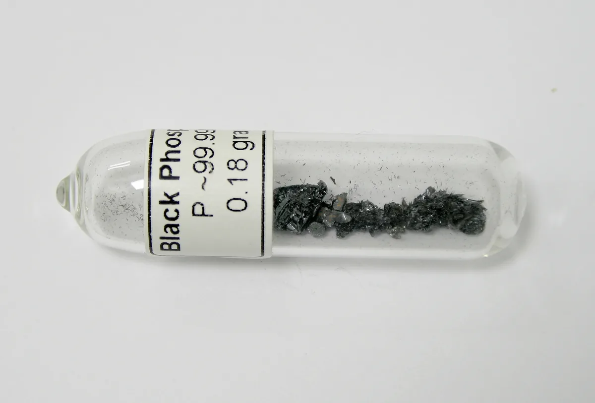
A sealed glass ampoule holding a few dark grey, metallic-looking crystals, with a label that begins “Black Phos” and reads 0.18 grams.
Black phosphorus, the layered crystal that phosphorene is peeled from, sealed in a glass ampoule that keeps air and moisture out. Image: Alshaer666, CC BY-SA 3.0; resized.

Key properties

  • Layer-dependent direct gap from ~0.3 eV (bulk) to ~2 eV (monolayer, quasiparticle)
  • Hole mobility up to ~1,000 cm2/(V·s) at room temperature in ~10 nm flakes
  • Strong in-plane anisotropy: effective mass, mobility, optical absorption and thermal conductivity all differ between armchair and zigzag
  • Monolayer exciton binding energy of several hundred meV, strongly dependent on the dielectric environment

How it is made

  • Mechanical exfoliation of bulk crystals, ideally inside a glovebox
  • Bulk crystals by high-pressure conversion of red phosphorus, or by low-pressure mineraliser-assisted transport with Sn and SnI4
  • Liquid-phase exfoliation in deoxygenated solvents – few-layer dispersions
  • Direct thin-film growth by pulsed laser deposition or CVD – early stage and poorly crystalline

Uses, and how close they are

  • Mid-infrared and polarisation-sensitive photodetectorsprototype
  • Anodes for lithium- and sodium-ion batteries (as composites)lab
  • Field-effect transistorslab

Readiness runs lab → prototype → pilot → deployed.

Open problems

  1. Can scalable, air-stable passivation be achieved without degrading mobility?
  2. Can crystalline black phosphorus films be grown directly at wafer scale?
  3. How do the anisotropic excitons evolve with layer number and dielectric environment?

Going deeper

Short notes for specialists. Choose a lens in the header and yours comes first.

For theoreticians · your lens

Interlayer coupling is unusually strong for a van der Waals material and drives the gap from ~2 eV to ~0.3 eV. PBE underestimates badly, and the choice of dispersion correction changes interlayer distances and therefore gaps, so use HSE or GW with converged k-grids. Excitons are large and anisotropic, and modest strain strongly modulates the gap.

For experimentalists · your lens

Handle and exfoliate in a glovebox and encapsulate before exposing to light in air. Determine crystal orientation with polarisation-resolved Raman: the A1g, B2g and A2g modes near 362, 439 and 467 cm−1 have angle-dependent intensities.

For engineers · your lens

Excellent infrared optoelectronic performance, but air instability and the lack of wafer-scale growth confine it to niche detectors at best; any product would need hermetic encapsulation.

In the research tracks

Recent news

The newest items tagged Phosphorene, from the news feed updated 5 Oct 2026.

Journal Nano Letters

Interfacing Two Topological Insulators, α -Bismuthene and β -Silicene, with a Rare-Earth Magnetic Monolayer

The integration of diverse electronic phenomena, such as magnetism and nontrivial topology, into a single low-dimensional system gives rise to unusual quantum effects. Here we combine two 2D topological insulators, α-bismuthene and β-silicene, with a Ho monolayer. Bismuthene is synthesized within a rarely realized…

Preprintnot yet peer reviewed arXiv

Screening of Coulomb Interactions in MoS2 Nanoribbons: Enhanced Coulomb interactions, Antiscreening, and Edge Magnetism

MoS2 has attracted significant attention for its promising applications in optoelectronics, owing to the remarkable stability of its excitons and trions. These quasiparticles have large binding energies that arise from the MoS2 moderate band gap and the unconventional screening of Coulomb interactions in low…

Journal Nano Letters

Anisotropic Quantum Hall Transport in a Black Phosphorus Two-Dimensional Hole Gas

Intriguing many-body ground states often emerge from quantum Hall systems, driven by electron–electron interactions. Among them, states breaking translational and rotational symmetries─manifested by anisotropic magnetotransport─can be stabilized by intrinsic band anisotropy. Here, we fabricate few-layer black…

TheoryExperimentPhosphorene

All 15 items tagged Phosphorene in the news feed  ·  RSS feed for Phosphorene

Key references

  1. Two new modifications of phosphorusBridgman · Journal of the American Chemical Society 36, 1344 (1914)cited by 810doi:10.1021/ja02184a002
  2. Black phosphorus field-effect transistorsLi et al. · Nature Nanotechnology 9, 372 (2014)cited by 8,459doi:10.1038/nnano.2014.35
  3. Phosphorene: an unexplored 2D semiconductor with a high hole mobilityLiu et al. · ACS Nano 8, 4033 (2014)cited by 6,511doi:10.1021/nn501226z
  4. Highly anisotropic and robust excitons in monolayer black phosphorusWang et al. · Nature Nanotechnology 10, 517 (2015)cited by 1,460doi:10.1038/nnano.2015.71