The most studied 2D semiconductor. As a single layer it becomes a direct-gap semiconductor that emits light and makes a transistor that switches properly on and off – what graphene cannot do. It is the leading candidate for ultra-thin transistor channels in future chips, and in bulk form it has been used for decades as a dry lubricant and a refinery catalyst.
Crystal structure
Drag to turn
They are coordination polyhedra. Only complete ones are drawn.
Three layers of 2H-MoS2, the usual form of molybdenite. Each layer is turned by 180° against the one below, so molybdenum sits over sulfur, and every second layer repeats: c = 12.30 Å, two layers per cell. A stack with an even number of layers has an inversion centre again; one with an odd number does not. Cell from Schönfeld, Huang and Moss, Acta Crystallographica B 39, 404 (1983); COD 9007660.
Three layers of 3R-MoS2. Each layer is shifted by the same step in the same direction, so sulfur sits over molybdenum and the pattern repeats only after three layers: c = 18.37 Å. No layer is the mirror image of its neighbour, so a 3R crystal has no inversion centre at any thickness, and its second-harmonic signal grows as layers are added. Cell from Schönfeld, Huang and Moss, Acta Crystallographica B 39, 404 (1983); COD 9007661.
Mo
S
Cell
Hexagonal, a = 3.16 Å
Atoms per cell
3
Mo–S bond
2.42 Å
Height
3.17 Å between the outer atom centres
A plane of molybdenum between two planes of sulfur. Upper and lower sulfur atoms sit directly above one another, so each Mo is inside a trigonal prism of six S atoms. A single layer has no inversion centre, which is why its K and K′ valleys can be addressed separately with circularly polarised light. Geometry of bulk 2H-MoS2 at room temperature: a = 3.16 Å, sulfur planes 1.59 Å above and below the Mo plane.
What it looks like
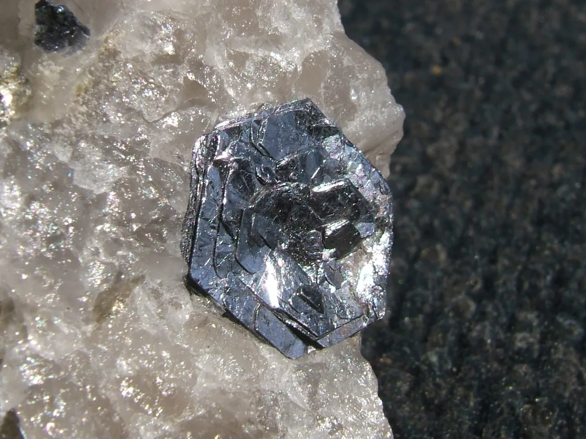
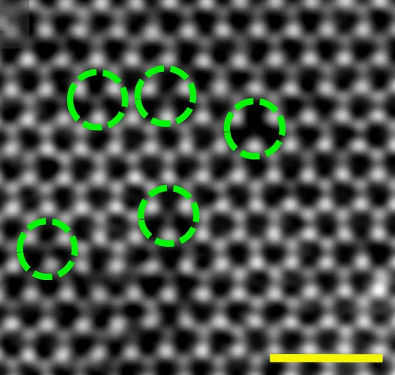
Molybdenite, the mineral form of MoS2, on quartz from the Molly Hill mine in Quebec. The crystal is 15 mm across, and its flat six-sided face is the top of the stack of layers. Image: John Chapman (Pyrope), CC BY-SA 4.0; resized.A single layer of MoS2 in a scanning transmission electron microscope. Each bright spot is a column of atoms seen end-on, and the circles mark sulfur sites where atoms are missing. Scale bar: 1 nm. Image: Jinhua Hong and colleagues, Nature Communications 6, 6293 (2015), CC BY 4.0; resized.
Key properties
Monolayer photoluminescence is roughly 104 times more efficient than bulk – the signature of the indirect-to-direct crossover
A and B excitons near 1.88 and 2.03 eV (monolayer, room temperature)
Room-temperature electron mobility typically 10–100 cm2/(V·s) in devices, limited by defects, interfaces and contacts
Valence-band spin–orbit splitting at K of ~150 meV; valley-selective excitation with circularly polarised light
Young’s modulus ~270 GPa; monolayers break at roughly 6–11% strain
Contact resistance as low as 42 Ω·µm with semimetallic antimony contacts (2023), after 123 Ω·µm with bismuth (2021)
How it is made
Mechanical exfoliation of natural molybdenite or synthetic crystals – reference flakes, although natural crystals carry many defects
CVD from MoO3 and sulfur at ~650–850 °C, often salt-assisted – triangular single-crystal domains that merge into polycrystalline films
MOCVD from Mo(CO)6 and a sulfur precursor – uniform wafer-scale monolayers
Epitaxy on vicinal sapphire with aligned domains – wafer-scale single-orientation films
Sulfurisation of pre-deposited Mo or MoO3 films – fab-friendly but polycrystalline
Lithium-intercalation or electrochemical exfoliation – solution-processable nanosheets, partly converted to the metallic 1T phase
Uses, and how close they are
Transistor channels for advanced logic and back-end-of-line circuitsprototype
Photodetectors and flexible optoelectronicsprototype
Electrocatalytic hydrogen evolution at edge siteslab
Dry lubricant and hydrodesulfurisation catalyst (bulk MoS2)deployed
Readiness runs lab → prototype → pilot → deployed.
Open problems
What limits mobility in wafer-scale films – chalcogen vacancies, grain boundaries, interface traps or remote phonons – and which of these can be engineered away?
Can a stable p-type MoS2, or a well-matched p-type partner, be achieved for complementary 2D logic?
How many reported ‘sulfur vacancies’ are really oxygen substitutions or antisite defects?
Going deeper
Short notes for specialists. Choose a lens in the header and yours comes first.
For theoreticians · your lens
Band edges at K are dominated by Mo d orbitals, so a three-band tight-binding model captures the valley physics; spin–orbit coupling splits the valence band by ~150 meV but the conduction band by only a few meV. PBE gets the direct monolayer gap right in character but wrong in size – GW–BSE with Coulomb truncation is needed for quasiparticle gaps and exciton binding energies (a few hundred meV, strongly screening-dependent). Defect studies must separate sulfur vacancies from substitutional oxygen, which look similar in STM but differ in their gap states.
For experimentalists · your lens
Count layers with Raman: the separation between E′ (~385 cm−1) and A′1 (~403–405 cm−1) is ~18–20 cm−1 in a monolayer and grows towards ~25 cm−1 in bulk (532 nm excitation). Confirm monolayers by strong PL at ~1.85–1.9 eV and by SHG, which is strong for odd and absent for even layer numbers in 2H stacking. A′1 responds to doping and E′ to strain, so do not infer layer number from peak positions alone on doped or strained samples.
For engineers · your lens
The most mature 2D semiconductor for integration: MOCVD delivers uniform wafer-scale monolayers, and 300 mm test transistors have been built in industrial research fabs. The hard problems are contact resistance (industry targets are around 100 Ω·µm), growth temperatures above back-end-of-line budgets (typically ≤400–450 °C), dielectric deposition on an inert basal plane, and the lack of a stable p-type counterpart.
Optoelectronic synaptic devices, particularly those based on two-dimensional (2D) transition metal dichalcogenides (TMDs), emulate biological synaptic functions, promising in neuromorphic computing. However, most TMD-based synapses rely on external gate or bias control, leading to complicated device architecture and…
Contact resistance remains a primary bottleneck in two-dimensional (2D) semiconductor field-effect transistors (FETs), yet the concurrent influence of metal work function, adhesion, and deposition temperature obscures the underlying mechanisms. Here, using bilayer MoS2 as a model system, we systematically benchmark…
One-dimensional transition metal dichalcogenides (TMD) nanoribbons (NRs) offer a promising route to aggressive channel-width scaling in nanoscale transistors. However, controlling their layer number, a key determinant of device performance, has remained elusive. Here, we demonstrate a chemical vapor deposition (CVD)…
Moiré superlattices formed in transition metal dichalcogenides (TMDs) offer a versatile platform for exploring emergent quantum phases arising from strong electronic correlations. In this work, we develop a new experimental platform, the quantum well resonant tunneling diode (QWRTD), to probe the electronic landscape…
Moiré superlattices formed in transition metal dichalcogenides (TMDs) offer a versatile platform for exploring emergent quantum phases arising from strong electronic correlations. In this work, we develop a new experimental platform, the quantum well resonant tunneling diode (QWRTD), to probe the electronic landscape…
Atomically thin MoS2: a new direct-gap semiconductorMak et al. · Physical Review Letters 105, 136805 (2010)cited by 15,430doi:10.1103/PhysRevLett.105.136805
Emerging photoluminescence in monolayer MoS2Splendiani et al. · Nano Letters 10, 1271 (2010)cited by 9,520doi:10.1021/nl903868w
Single-layer MoS2 transistorsRadisavljevic et al. · Nature Nanotechnology 6, 147 (2011)cited by 14,996doi:10.1038/nnano.2010.279
High-mobility three-atom-thick semiconducting films with wafer-scale homogeneityKang et al. · Nature 520, 656 (2015)cited by 1,963doi:10.1038/nature14417
Ultralow contact resistance between semimetal and monolayer semiconductorsShen et al. · Nature 593, 211 (2021)cited by 1,414doi:10.1038/s41586-021-03472-9
Approaching the quantum limit in two-dimensional semiconductor contactsLi et al. · Nature 613, 274 (2023)cited by 620doi:10.1038/s41586-022-05431-4